Semiconductor inspection light source for fluorescence microscopy
Fluorescence microscopy is a powerful tool widely used in semiconductor inspection for various purposes, including defect detection, material characterisation, and quality control.
In semiconductor inspection, fluorescence microscopy leverages the fluorescent properties of certain materials to enhance contrast and reveal specific features that may not be visible with traditional bright-field microscopy techniques.
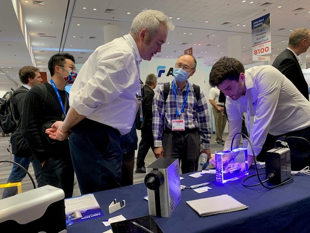
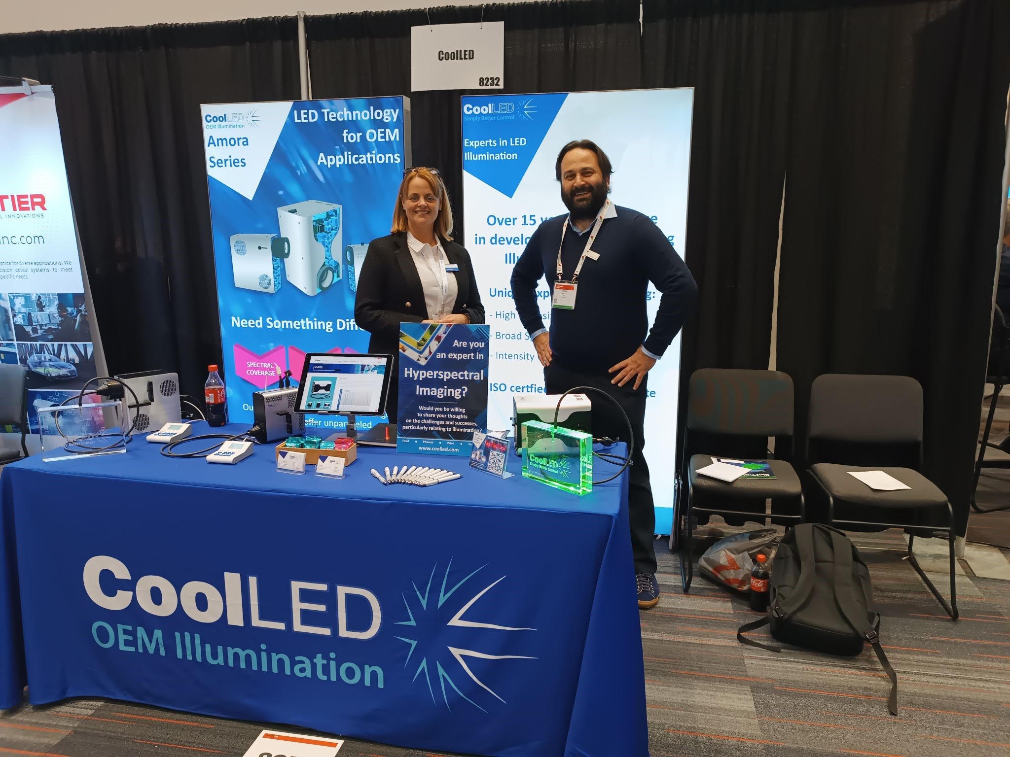
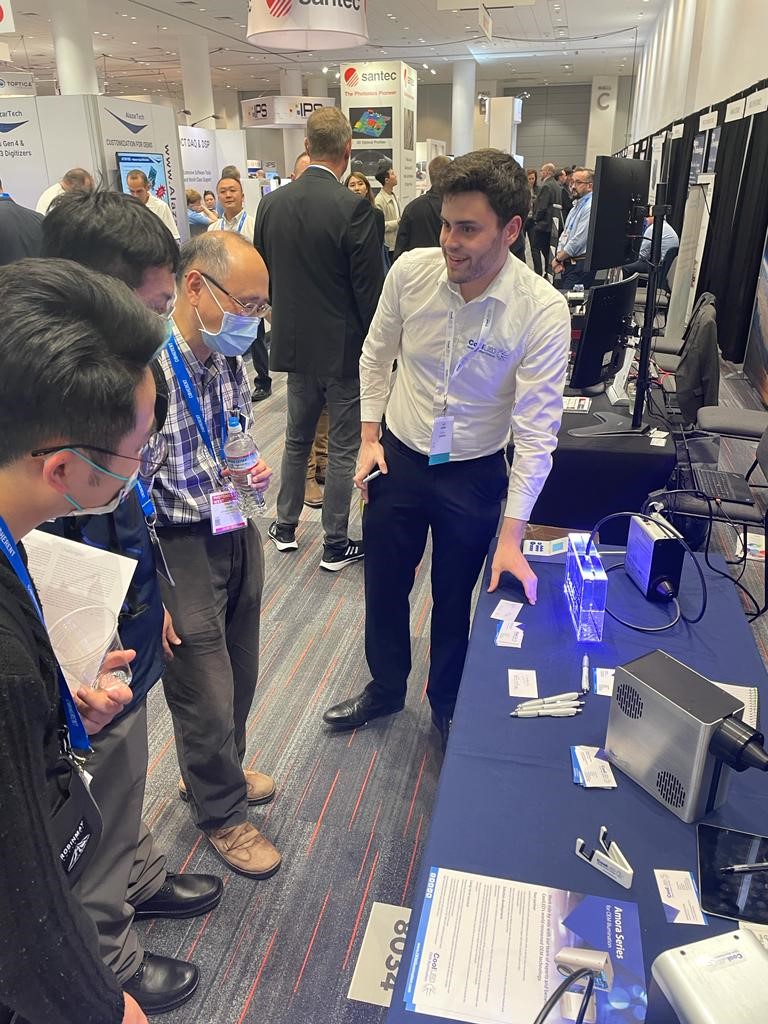
CoolLED for Fluorescence Illumination
We design and manufacture cutting edge LED illuminators using the very latest in LED technology. Our fast-growing company is based in Hampshire, UK, and our unparalleled technical expertise is founded on optical engineering and mechanical design.
We have led the way in transforming light source technology since our team of four introduced the first commercially available LED illuminator in 2006. Initially answering the highly demanding requirements of the life science microscopy industry, we now also design powerful and stable LED illuminators for a range of applications in the material sciences and industrial inspection arena.
At CoolLED, we understand the critical role that high-quality light sources play in semiconductor inspection processes. That’s why we offer a customised platform for the semiconductor inspection light source designed to optimise your inspection procedures with precision and accuracy.
UK : +44 (0)1264 323040
Call Us Now – We’re Here To Help
When calling it would be useful to have the following information:
Your Name
Company Name (If Applicable)
Email Address
Your OEM Illumination Requirements
Request A Callback
Why Choose LEDs for the Semiconductor Inspection Light Source?
When it comes to the semiconductor inspection light source, the illumination technology has come a long way since mercury and metal halide lamps. LED technology has now taken centre stage for a range of reasons:
Stability: Irradiance declines over the lifetime of a mercury or metal halide lamp, whereas LEDs are much more stable over time.
Control: LEDs can be easily controlled. They can be switched on and off with precise microsecond timing, and LED irradiance can also be modulated electronically. Moreover, control can be achieved within software for seamless integration into the complete inspection system.
Speed: Another advantage of solid-state LED illumination is the speed of electronic control, where triggering is in the order of micro-seconds. Removing the need for a mechanical shutter further improves imaging speed, increasing inspection times and therefore the throughput of the inspection workflow.
Up-time: Lamps frequently need replacing, whereas LEDs are long-lived. This maximises up-time of the system in the inspection workflow.
Safety and the environment: Mercury in lamps is hazardous to people and the environment. In addition to this, LEDs are more energy efficient and emit much less heat.
Partnering with Solid-State OEM Illumination Experts
At CoolLED, we take pride in our ability to guide our partners and work together to create custom solid-state OEM illumination solutions. We understand that each project requires a unique approach, and our team of experts is dedicated to working closely with you to develop tailored solutions that align with your specific requirements.
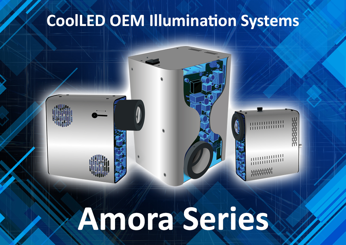
The CoolLED Solution: Place the Amora at the Heart of Your Semiconductor Inspection
The CoolLED Amora platform represents a cutting-edge approach to LED illumination technology tailored to individual applications requirements across the semiconductor inspection workflow. Designed to meet the demands of modern industrial optical inspection environments, the Amora platform offers a range of features and benefits that set it apart from traditional illumination systems.
At the core of the Amora platform is its emphasis on proven performance and innovation. By leveraging off-the-shelf technology, CoolLED minimises development risks while maximising innovation, enabling faster product development cycles and tighter timelines. This approach ensures that manufacturers can integrate the latest LED illumination technology into their semiconductor inspection system with confidence, knowing that they are backed by a proven track record of success.
Supported by the Experts
In addition to its performance and flexibility, the Amora platform is backed by CoolLED’s team of experts who provide unparalleled support and guidance throughout the development process. From initial design consultations to ongoing technical support, CoolLED’s team is dedicated to helping users get the most out of their Amora-based illumination solutions.
Overall, the CoolLED Amora platform represents a significant advancement in LED illumination technology for semiconductor inspection applications. With its focus on proven performance, innovation, flexibility, and expert support, the Amora platform is poised to revolutionise the way manufacturers approach fluorescence microscopy in optical industrial inspection.
Why Work with CoolLED?
Our semiconductor inspection light sources are engineered using state-of-the-art technology and the highest quality materials to ensure optimal performance and reliability. Whether you require optical stability, uniform illumination, precise wavelength control, or high-speed triggering, our light sources deliver consistent and reliable results every time.
Custom solutions to fit your unique requirements: We recognise that every semiconductor inspection application is unique. That’s why we have optimised the Amora platform to achieve unmatched flexibility, allowing manufacturers to tailor their illumination solutions to meet the specific requirements of their applications. Whether selecting from a range of LED wavelengths, selecting a bespoke light output coupling, or even a specialised coating for the light source housing, CoolLED’s Amora platform can be highly customised. Our team of experts will work closely with you to design a solution that perfectly aligns with your needs and ensure optimal performance and compatibility with any optical inspection setup.
Exceptional reliability and durability: Reliability is paramount in semiconductor inspection environments. That’s why our semiconductor inspection light sources are built to withstand the rigors of industrial use. With robust construction and advanced thermal management systems, our light sources ensure long-term reliability and durability, minimising downtime and maximising productivity.
Industry-leading innovation: At CoolLED, we are committed to staying at the forefront of technological innovation. Our dedicated research and development team continuously explores new advancements in semiconductor lighting technology to bring you the latest innovations and improvements in semiconductor inspection performance. Driven by a passion for progress, we continuously push the boundaries of what’s possible, seeking out new breakthroughs that redefine the landscape of semiconductor inspection performance. By harnessing the latest advancements in semiconductor technology, we empower your organisation with unparalleled tools and capabilities, providing you with a distinct competitive advantage in today’s dynamic market.
Expert support and service: From the initial consultation, we provide comprehensive support and service to ensure that your semiconductor inspection light sources perform optimally throughout their lifespan. This also includes a full testing and reporting service, where our team of experts provide full testing and prototypes, while interpreting complex optical data and providing comprehensive performance reports. When it comes to ongoing maintenance and support, our team is always available to assist you every step of the way.
Contact Us Today
Contact us today to learn more about our semiconductor inspection light sources and discover how we can help enhance the performance and efficiency of your semiconductor inspection processes.
We needed a branded offering to package with our range of microscopy cameras. CoolLED has worked with us to deliver a solution which is simple to demonstrate and sell while complementing our own market leading products. They have also worked with our purchasing, logistics and support teams to ensure a quality experience for us and most importantly, our customers.
Mathieu Frechin
Head of Quantitative Biology, Nanolive
We received a CoolLED Illumination System prototype which was integrated and tested over February 2017. The first microscope with a CoolLED Illumination System was sold just later that year. In addition to meeting technical specifications, CoolLED was very quick to react to changes in our situation and provide appropriate solutions.
Leigh Rees
General Manager, Aurox
CoolLED has provided Aurox with an OEM version of the popular and versatile pE-300ultra that mechanically, optically and electronically integrates with Aurox’s new Unity. The powerful pE-300ultra Light Source sits directly inside the casing of Unity and enables full control of intensity and switching from within Unity’s software. CoolLED is a valued partner in our supply chain, providing excellent levels of service and support at all stages. We have developed a high degree of trust and a seamless working relationship.
Kai Reiser
Purchasing Manager & Confidential Clerk of Medipan and GA Generic Assays, Medipan GMBH
Medipan has used CoolLED LED Illumination Systems for many years. The ability to control the excitation intensity of our assays for sample analysis has been crucial for the successful performance of our Aklides system. Instant on/off control through our system software means that illumination is fully integrated with the product. CoolLED has worked closely with Medipan as we have developed our products to ensure compatibility and performance. A responsive helpful supplier allows our scientists and engineers to focus on our core capabilities when developing products for the life sciences.
Andor has worked with CoolLED to transition multiple product lines to the use of LED illumination in place of older technologies. This allows us to take advantage of new levels of illumination stability and synchronised device control to enhance our products in a competitive market place. As well as meeting stringent worldwide compliance needs, CoolLED has also been extremely reactive to our specific needs when it comes to optimisation of their solution to our hardware and therefore target applications.