Tips for designing and manufacturing an LED light source for an automated imaging system
Embarking on designing and manufacturing a new automated imaging system for fluorescence is a challenge in a competitive market and can quickly become expensive.
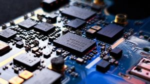 For many of the components integral to the microscope, it is simply not feasible to manufacture these in-house. However, the function of the light source can seem relatively simple: provide a focused beam of light at a specified wavelength. In fact, you might imagine that it is entirely possible to minimise build costs and bring the design and manufacture of this component in-house.
Catalogues have countless LEDs to choose from, which are becoming increasingly powerful and provide users with many additional benefits compared to traditional lamps (see Why LED Illumination). For these reasons, LEDs have become the go-to light source on modern automated imaging systems, as manufacturers future-proof their products. Depending on the application of the system, you can pick the exact wavelength range required for compatible fluorophores. Combined with the accessibility of customised 3D printed components and in-house engineering resource, a cost-effective solution might be feasible. But what are the trade-offs to consider?
Precision: Each production round of LED manufacture results in performance deviations, including wavelength and light output. Purchasing low quantities of LED chips directly from a component reseller means you have a ‘lucky dip’ with LEDs from different bins – for example, we have experienced wavelength variance of up to 25 nm. This spread is typically under 5 nm for established LED microscope light source manufacturers who buy in bulk directly from the manufacturer at bare LED die level, and perform internal testing.
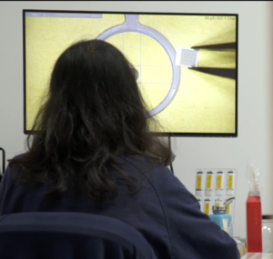
Performance: Unfortunately, fluorescence microscopy illumination is not so simple. The light hitting the sample plane must be both powerful and homogenous. Then consider control: for example, fast triggering speeds are crucial for reducing sample exposure, synchronising imaging times and analysing live samples. Percentage irradiance modulation and stability is equally important, and the electronic engineering involved can be highly complex.
Lifetime: Automated imaging systems, especially in biomedical applications, work their components hard. Samples can be running around the clock with many millions of images acquired per year. Maximising both the lifetime and power of LEDs requires sophisticated thermal management, and this has a significant impact on performance. Once again, this is a highly demanding area of expertise and (as you can tell from the company name) – one that CoolLED specialises in! We are ‘cool’ but the name emphasises the work done on keeping our LEDs cool too!
Risk: Manufacturing a light source in-house that matches the performance expected of the latest systems is a complex task. With this complexity comes a high level of risk which may impact the product development timeline – and more critically the reliability of the light source and therefore the entire system over time. Our team of specialised engineers work hard to reduce risk by working with the established CoolLED Amora platform and adapting it to each set of requirements, and prototypes can be ready in just weeks. Once the product is released, outsourcing further reduces risk where LEDs are covered by warranty, and any ongoing maintenance can be addressed quickly to maximise uptime.
At CoolLED, we have OEM focused engineers who are ready to work closely with you at the earliest stage in your development project so that the custom microscopy illumination aspect is one less detail to worry about.


